Omega4 Hardware Design Guide
This guide provides electrical and layout recommendations for integrating the Omega4 (OM-O4) module into a custom carrier board.
Download design libraries
Download the package library files for your CAD tool:
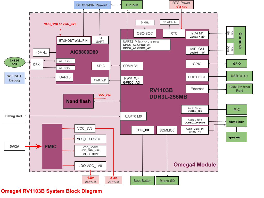
2. System Block Diagram
3. Pin Definition
3.1 Pin Assignment
The table below lists the Omega4 module pins and their common alternate functions. In the I/O column, I indicates input, O indicates output, and I/O indicates bidirectional.
All MIPI-related pins on Omega4 use 1.8 V logic. Add level shifting if you need to interface to 3.3 V peripherals.
Left (Pins 1-21)
| No | Pin Name | I/O | Description |
|---|---|---|---|
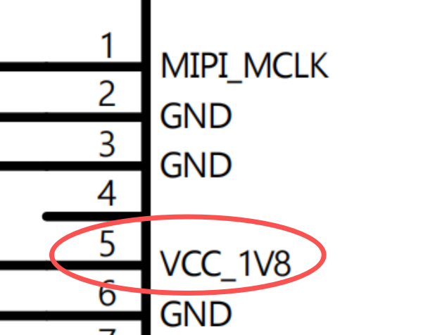
| 1 | CAM_CLK0_OUT/ | I/O | MIPI_MCLK (1.8 V) |
| 2 | GND | I | GND |
| 3 | GND | I | GND |
| 4 | NC | NC | |
| 5 | VCC_1V8 | O | VCC_1V8, 1.8 V output (max 100 mA) |
| 6 | GND | I | GND |
| 7 | SDMMC0_DET/ | I/O | SDMMC_DET |
| 8 | SDMMC0_D1/ | I/O | SDMMC_D1 |
| 9 | SDMMC0_D0/ | I/O | SDMMC_D0 |
| 10 | SDMMC0_CMD/ | I/O | SDMMC_CMD |
| 11 | SDMMC0_CLK/ | I/O | SDMMC_CLK |
| 12 | SDMMC0_D3/ | I/O | SDMMC_D3 |
| 13 | SDMMC0_D2/ | I/O | SDMMC_D2 |
| 14 | GND | I | GND |
| 15 | USB_DM | I/O | USB_DM |
| 16 | USB_DP | I/O | USB_DP |
| 17 | GND | I | GND |
| 18 | ACODEC_AVSS | I | ACODEC_AVSS |
| 19 | ACODEC_LINEOUT | O | LINE_OUT |
| 20 | GND | I | GND |
| 21 | GND | I | GND |
Bottom (Pins 22-56)
| No | Pin Name | I/O | Description |
|---|---|---|---|
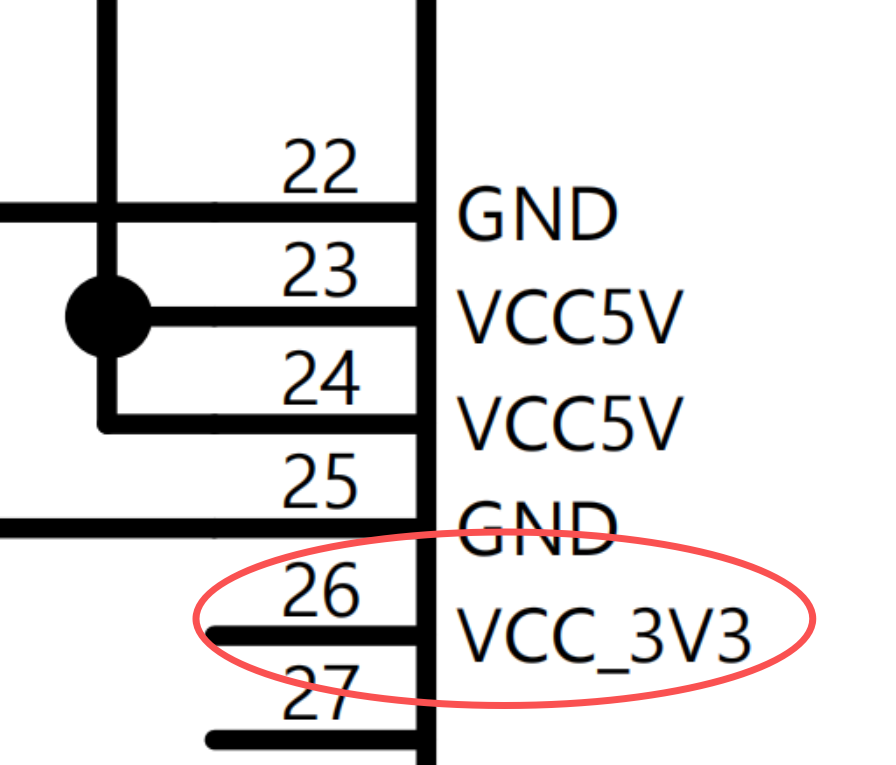
| 22 | GND | I | GND |
| 23 | 5 V input | I | 5 V main power input |
| 24 | 5 V input | I | 5 V main power input |
| 25 | GND | I | GND |
| 26 | VCC_3V3 | O | VCC_3V3, 3.3 V output (max 100 mA) |
| 27 | NC | / | NC |
| 28 | VCC_RTC | I | VCC_RTC, input power < 3.63 V |
| 29 | FSPI_D0 | I | FSPI_D0, boot key |
| 30 | GND | I | GND |
| 31 | ACODEC_MIC_N | I | AUD_MICIN |
| 32 | ACODEC_MIC_P | I | AUD_MICIP |
| 33 | ACODEC_MICBIAS | ACODEC_MICBIAS | |
| 34 | GND | I | GND |
| 35 | PWM0_CH0_M0/ | I/O | GPIO0_A1_d |
| 36 | RTC_32K_CLKO/ | I/O | GPIO0_A0_z |
| 37 | PWM0_CH3_M0/ | I/O | PWM0_CH3_M0/GPIO0_A2_d |
| 38 | PWR_CTRL_M1/ | I/O | PWR_CTRL_M1/GPIO0_A4_d |
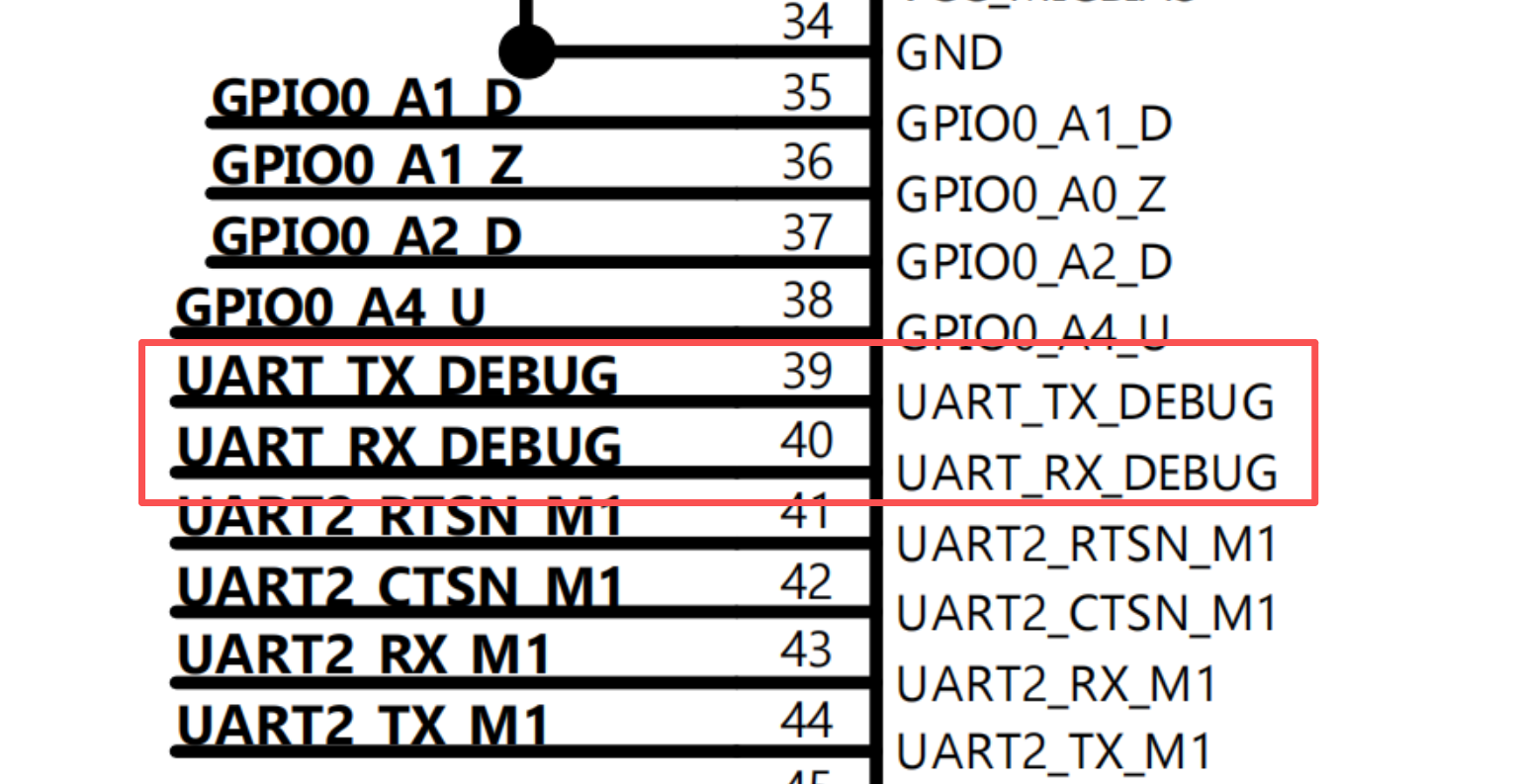
| 39 | UART0_TX_M0/ | I/O | SOC UART0_TX_M0 Debug |
| 40 | UART0_RX_M0/ | I/O | SOC UART0_RX_M0 Debug |
| 41 | UART2_RTSN_M1/ | I/O | UART2_RTSN_M1 |
| 42 | UART2_CTSN_M1/ | I/O | UART2_CTSN_M1 |
| 43 | UART2_RX_M1/ | I/O | UART2_RX_M1 |
| 44 | UART2_TX_M1/ | I/O | UART2_TX_M1 |
| 45 | BT_UART_RX (GPIOA4) | Wi-Fi/BT Dedicated | Wi-Fi/BT module pin, BT_UART_RX |
| 46 | BT_UART_TX (GPIOA5) | Wi-Fi/BT Dedicated | Wi-Fi/BT module pin, BT_UART_TX |
| 47 | BT_UART_CTS (GPIOA6) | Wi-Fi/BT Dedicated | Wi-Fi/BT module pin, BT_UART_CTS |
| 48 | BT_UART_RTS (GPIOA7) | Wi-Fi/BT Dedicated | Wi-Fi/BT module pin, BT_UART_RTS |
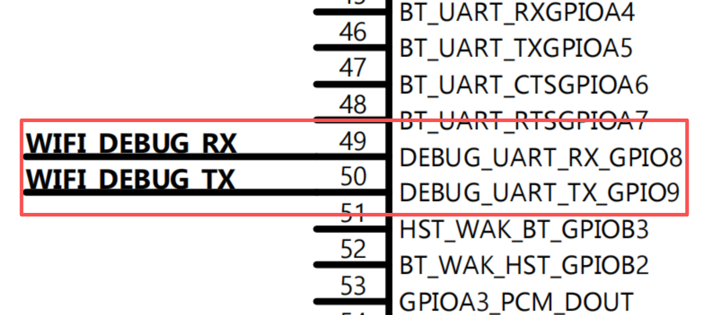
| 49 | WIFI Debug UART RX (GPIOA8) | Wi-Fi/BT Dedicated | Wi-Fi/BT module pin, debug UART RX |
| 50 | WIFI Debug UART TX (GPIOA9) | Wi-Fi/BT Dedicated | Wi-Fi/BT module pin, debug UART TX |
| 51 | HST_WAK_WF (GPIOB0) | Wi-Fi/BT Dedicated | Wi-Fi/BT module pin, host wake Wi-Fi |
| 52 | WF_WAK_HST (GPIOB1) | Wi-Fi/BT Dedicated | Wi-Fi/BT module pin, Wi-Fi wake host |
| 53 | PCM_DOUT (GPIOA3) | Wi-Fi/BT Dedicated | Wi-Fi/BT module pin, PCM data output |
| 54 | PCM_CLK (GPIOA1) | Wi-Fi/BT Dedicated | Wi-Fi/BT module pin, PCM clock |
| 55 | PCM_FSYNC (GPIOA0) | Wi-Fi/BT Dedicated | Wi-Fi/BT module pin, PCM frame sync |
| 56 | PCM_DIN (GPIOA2) | Wi-Fi/BT Dedicated | Wi-Fi/BT module pin, PCM data input |
Top (Pins 57-91)
| No | Pin Name | I/O | Description |
|---|---|---|---|
| 57 | GND | I | GND |
| 58 | Wi-Fi/BT Antenna | Wi-Fi/BT Dedicated | Wi-Fi/BT 2.4/5 GHz antenna |
| 59 | GND | I | GND |
| 60 | NC | / | NC |
| 61 | UART1_RX_M2/ | I/O | GPIO2_A7_d |
| 62 | UART1_TX_M2/ | I/O | GPIO2_A6_d |
| 63 | SARADC_IN0/ | I/O | SARADC_IN0/GPIO2_B4_z |
| 64 | GND | I | GND |
| 65 | FEPHY_TXP | O | FEPHY_TXP |
| 66 | FEPHY_TXN | O | FEPHY_TXN |
| 67 | GND | I | GND |
| 68 | FEPHY_RXP | I | FEPHY_RXP |
| 69 | FEPHY_RXN | I | FEPHY_RXN |
| 70 | GND | I | GND |
| 71 | MIPI_CSI_D3N/ | I/O | MIPI_D3N (1.8 V) |
| 72 | MIPI_CSI_D3P/ | I/O | MIPI_D3P (1.8 V) |
| 73 | GND | I | GND |
| 74 | MIPI_CSI_CK1N/ | I/O | MIPI_CLK1N (1.8 V) |
| 75 | MIPI_CSI_CK1P/ | I/O | MIPI_CLK1P (1.8 V) |
| 76 | GND | I | GND |
| 77 | MIPI_CSI_D2N/ | I/O | MIPI_D2N (1.8 V) |
| 78 | MIPI_CSI_D2P/ | I/O | MIPI_D2P (1.8 V) |
| 79 | GND | I | GND |
| 80 | MIPI_CSI_D1N/ | I/O | MIPI_D1N (1.8 V) |
| 81 | MIPI_CSI_D1P/ | I/O | MIPI_D1P (1.8 V) |
| 82 | GND | I | GND |
| 83 | MIPI_CSI_CK0N/ | I/O | MIPI_CKN (1.8 V) |
| 84 | MIPI_CSI_CK0P/ | I/O | MIPI_CKP (1.8 V) |
| 85 | GND | I | GND |
| 86 | MIPI_CSI_D0N/ | I/O | MIPI_D0N (1.8 V) |
| 87 | MIPI_CSI_D0P/ | I/O | MIPI_D0P (1.8 V) |
| 88 | GND | I | GND |
| 89 | PWM0_CH2_M2/ | I/O | MIPI_I2C_SDA (1.8 V) |
| 90 | PWM0_CH1_M2/ | I/O | MIPI_I2C_SCL (1.8 V) |
| 91 | CAM_CLK1_OUT/ | I/O | MIPI_RST (1.8 V) |
Pins marked Wi-Fi/BT Dedicated are connected to the Wi-Fi/Bluetooth module, not the main SoC. Although they are exposed on module pads, they are not accessible as system GPIO and should not be used as carrier-board GPIO signals.
4. Hardware Integration Guide
Power and Boot
4.1 5 V Power Supply
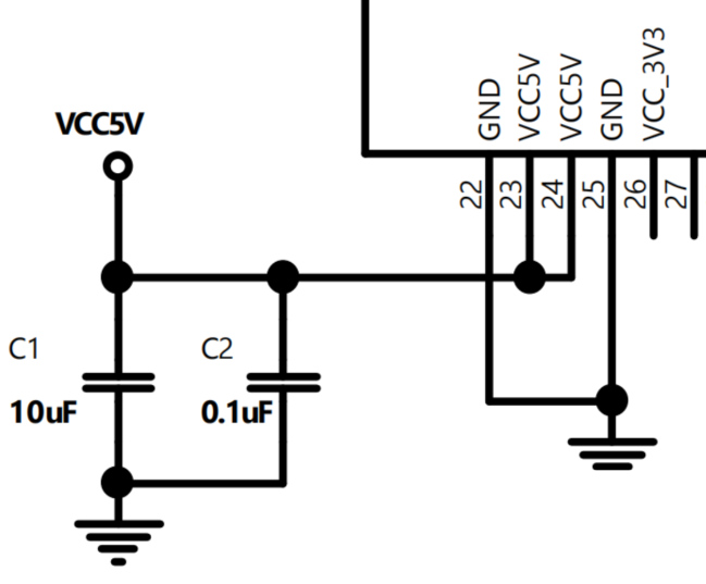
Provide a regulated 5 V supply to Omega4. PIN23 and PIN24 are the 5 V main power inputs; connect both pins to the 5 V rail.
Place one 10 uF bulk capacitor and one 0.1 uF high-frequency decoupling capacitor close to the power pins, with a short, low-impedance return to ground.
4.2 3.3 V and 1.8 V Power Output
Omega4 provides one 1.8 V output (PIN5) and one 3.3 V output (PIN26) for external peripherals. These rails are intended for light loads:
- VCC_1V8 (PIN5): up to 100 mA
- VCC_3V3 (PIN26): up to 100 mA
Do not exceed 100 mA on either rail to avoid impacting the module's internal power rails. For higher-current devices, generate the required supplies on the carrier board.
For camera designs, see Section 4.7 for MIPI-CSI 1.8 V signaling and level-shifting guidance.
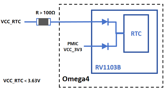
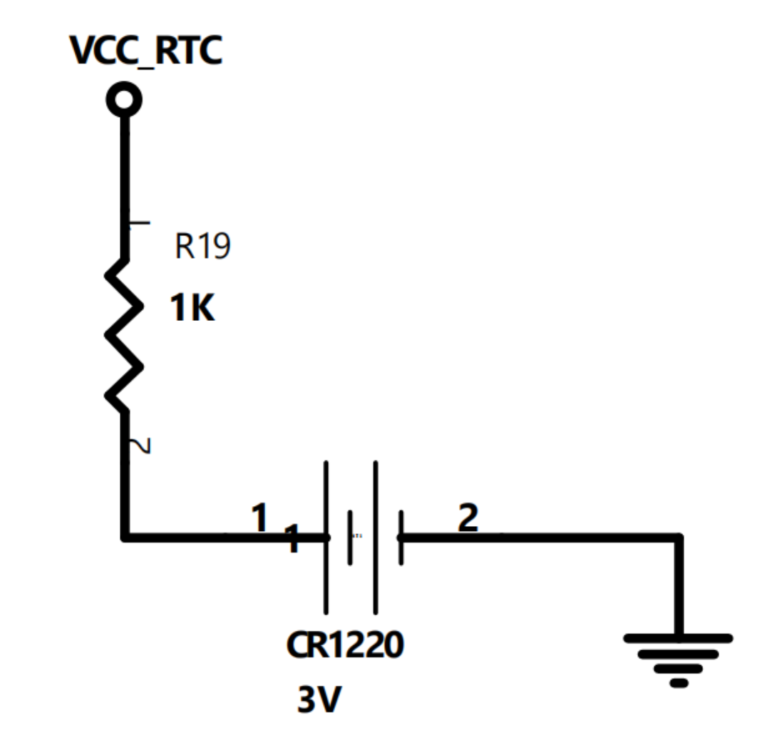
4.3 RTC Power Input
RV1103B integrates a dual-channel diode path from VCC_3V3 and VCC_RTC (PIN28). The RTC module can automatically select the active power source. It is recommended to connect VCC_RTC (PIN28) to an external supply such as a coin cell or lithium battery.
VCC_RTC requires a series resistor of 100 Ω or higher.
The RTC input is rated to a maximum of 3.63 V, so it cannot connect directly to a lithium battery (3.7 V to 4.2 V). Use a series resistor (for example 390 kΩ) to drop the voltage before using it as VCC_RTC.
4.4 Pins That Affect System Boot
PIN29 (FSPI_D0) is sampled during boot. If this pin is held low, the module enters MaskROM programming mode for recovery and firmware flashing.
You can connect FSPI_D0 to a momentary button (to ground) or expose it as a test point. Ensure the signal is not unintentionally pulled low during normal operation.
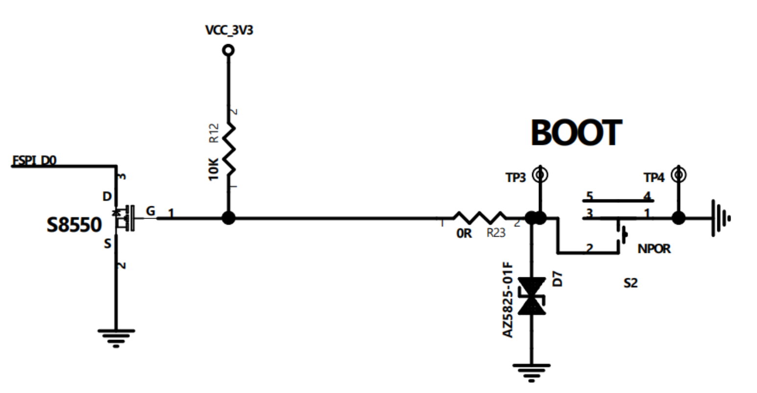
If your design does not require a button, reserve a test point instead. This simplifies factory test and field recovery.
4.5 Debug UART
The system default debug UART is RV1103B UART0 M0 on PIN39 (TX) and PIN40 (RX). The Wi-Fi chip also provides a debug UART on PIN49 and PIN50.
If the product does not require a UART header, reserve test points so it is easier to perform factory testing or issue commands during FCC/CE certification.
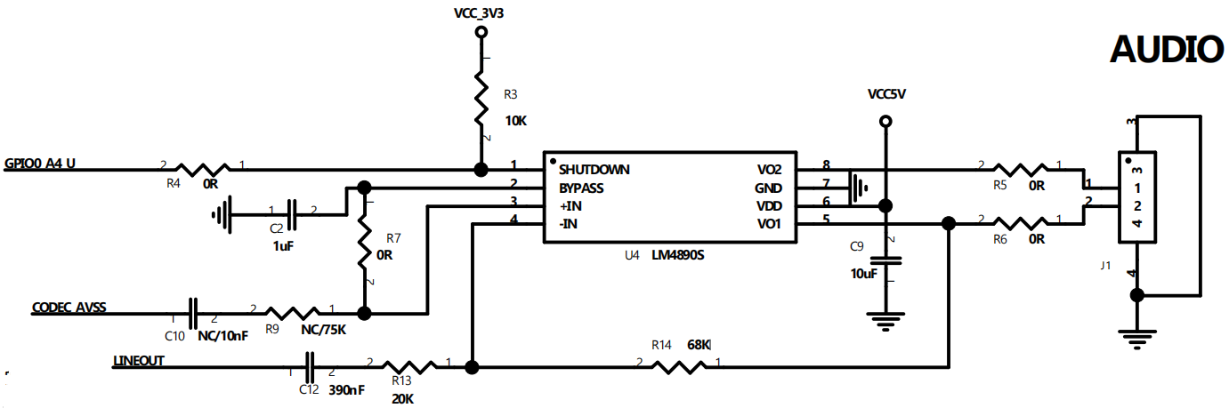
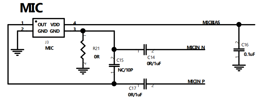
4.6 Audio & MIC
The built-in ACODEC of the RV1103B provides:
- One line-out output on PIN19.
- One differential MIC input on PIN31 and PIN32.
ACODEC_AVSS (PIN18) can be combined with Lineout to form a pseudo-differential signal. This can connect to the input of an external differential power amplifier (PA) for improved audio output.
High-Speed and RF
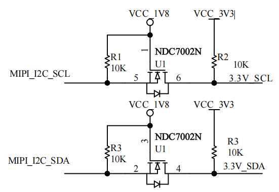
4.7 MIPI-CSI Pin Voltage
The MIPI-CSI pins use 1.8 V logic. If you need to interface to 3.3 V devices, add level shifting.
Use case: If your design uses Omega4's MIPI_I2C to control a 3.3 V I2C peripheral, add a bidirectional I2C level shifter. A reference circuit is shown below:
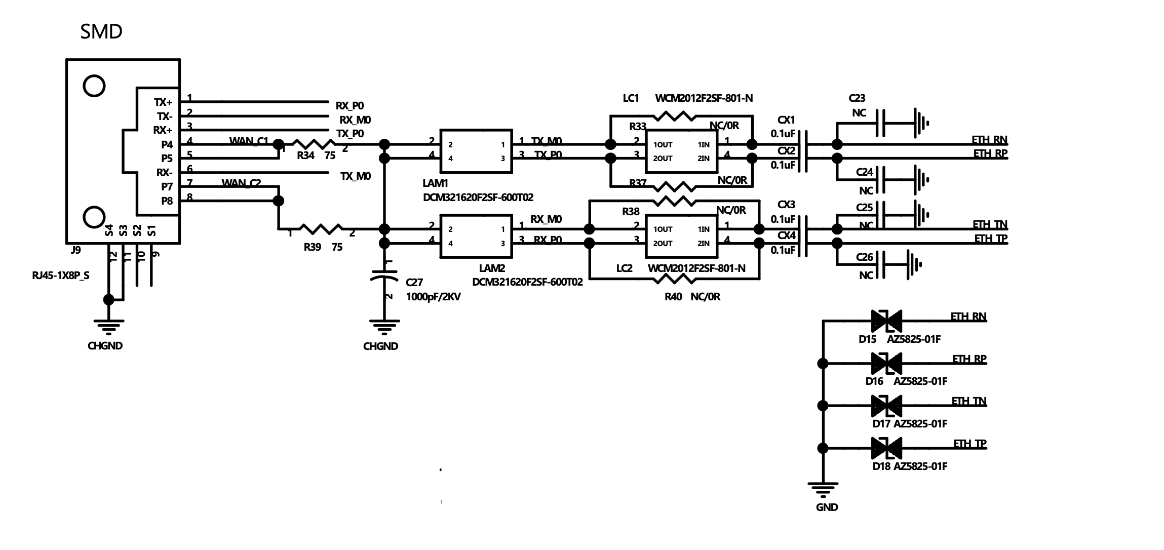
4.8 Ethernet Port
Reference circuit: You can use either an Ethernet jack with integrated magnetics or a standard Ethernet jack with external magnetics. The example below shows an implementation with external magnetics.
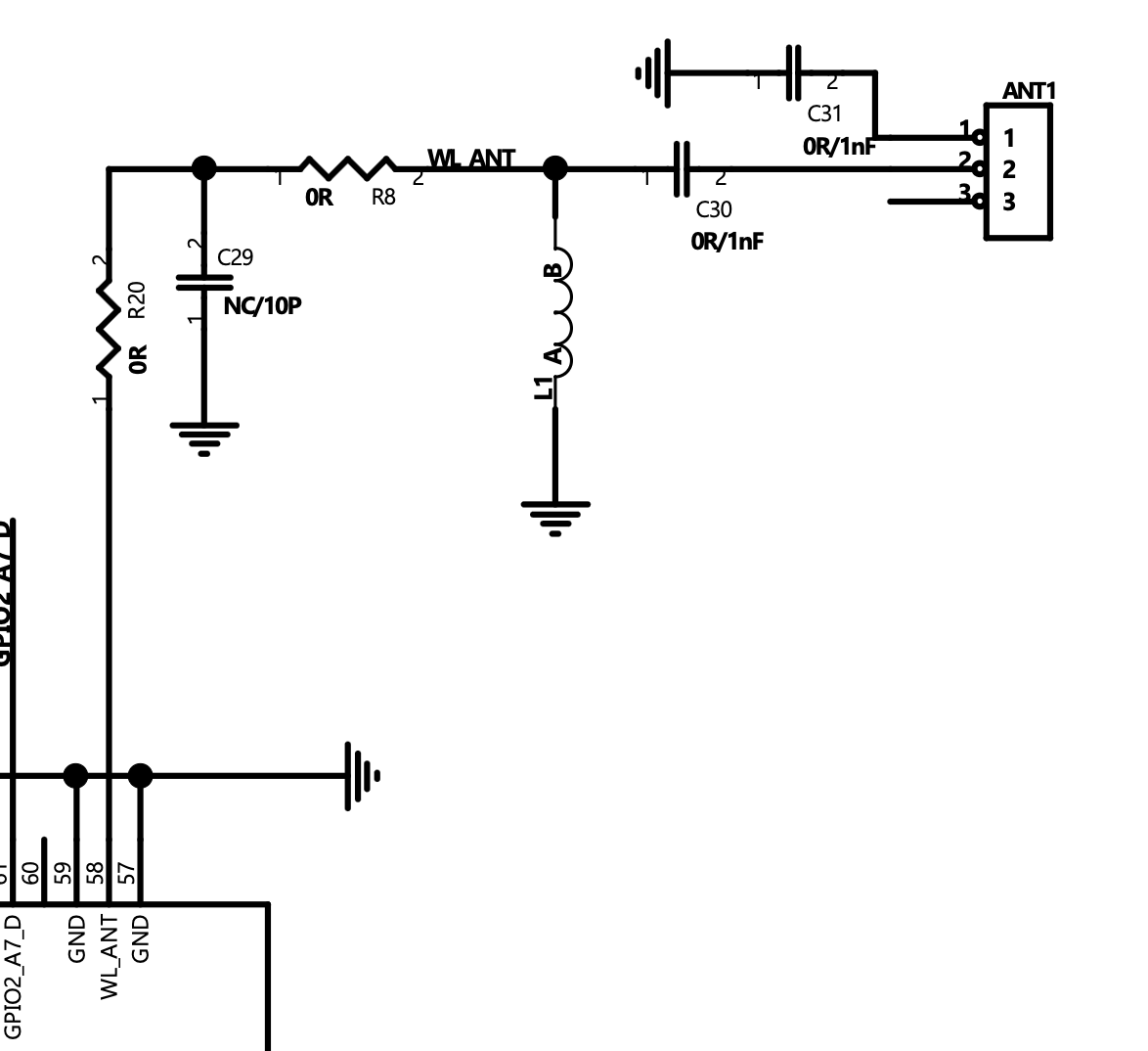
4.9 Antenna Design
The Omega4 EVB uses the OA-W03 SMD ceramic antenna. You can use an equivalent dual-band Wi-Fi antenna in your own design, as long as the RF layout, matching network, and validation are completed for the selected antenna. The OA-W03 is a compact 2.4 GHz / 5 GHz SMD ceramic antenna intended for Wi-Fi applications, with a small footprint and good radiation efficiency.
Connect the antenna feed to WL_ANT (PIN58) through the RF matching network.
Reference: OA-W03 datasheet.
4.9.1 OA-W03 Key Specifications
| Parameter | Value |
|---|---|
| Frequency | 2400–2500 MHz / 5200–5800 MHz |
| Impedance | 50 Ω |
| Gain | ~2 dBi at 2.4 GHz, ~4.9 dBi at 5 GHz |
| VSWR | < 2 |
| Size | 3.2 x 1.6 x 1.0 mm |
4.9.2 Layout Guidelines
-
Place the antenna at the edge of the PCB.
-
Keep a clearance area of approximately 6.2 x 4.6 mm free of ground and routing.
-
Use a 50 Ω controlled-impedance feed line.
-
Keep the feed trace short and straight.
-
Avoid placing a ground plane directly under the antenna.
4.9.3 Matching Network
Include a π-type matching network near the antenna feed. Use the following values as a reference starting point:
| Position | Reference Value |
|---|---|
| Series | 1.5 pF / 0.75 pF / 0 Ω |
| Shunt | 2 nH / NC |
Final component values must be tuned on the target PCB.
4.9.4 Design Notes
- Keep metal parts and components away from the antenna area.
- Optimize the layout with the final enclosure in place.
- Perform impedance tuning and RF validation during bring-up.
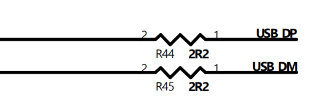
4.10 USB 2.0
The USB port supports both Host and Device modes. During normal operation, the USB port defaults to Device mode. It can be switched to Host mode via software commands or the BOOT button.
To improve signal integrity, place a 2.2 Ω series resistor on both USB DP and DM.
If the product does not need the USB port, reserve test points so it is easier to upgrade Omega4 firmware.
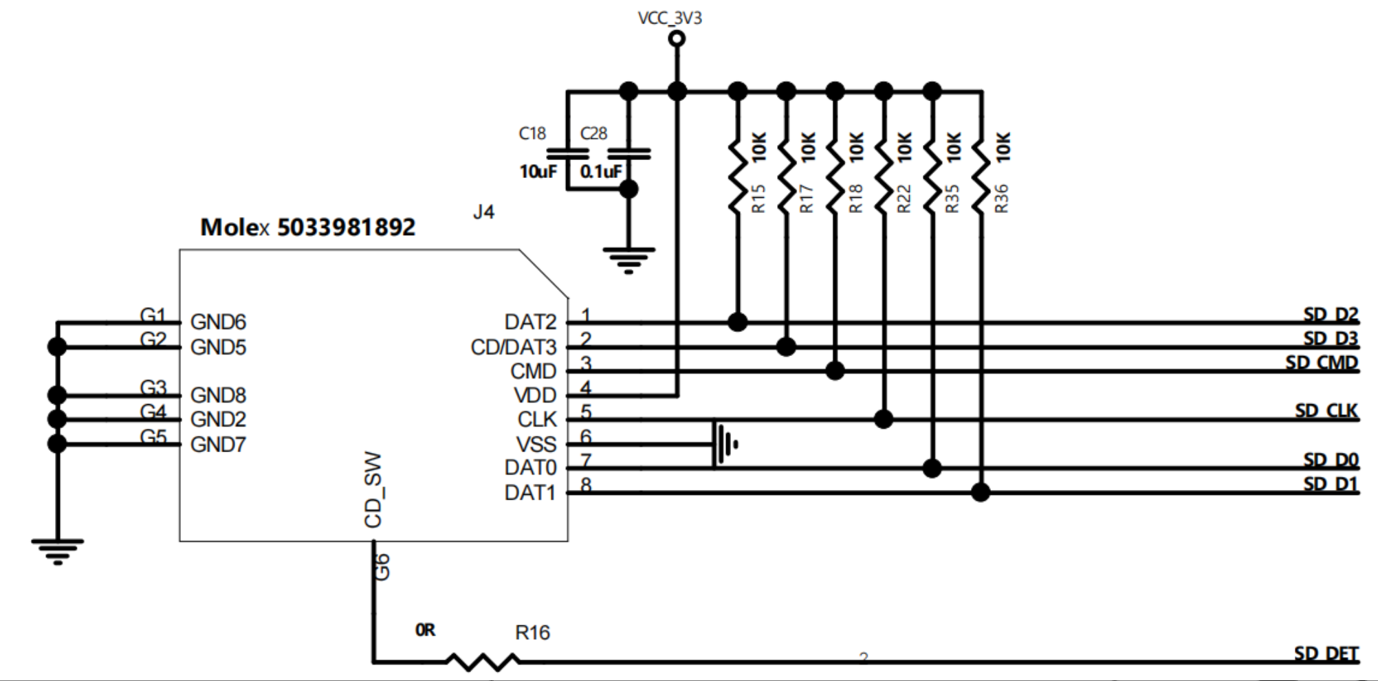
4.11 Extended Storage
Omega4 exposes an SDIO interface and can support Micro SD, SD NAND flash, or eMMC as extended storage.
Add pull-up resistors to the SDIO signals as required by your chosen storage device. A typical value is 10 kOhm.
4.11.1 Micro SD Card
Use the card-detect pin (SD_DET) to detect whether a card is inserted.
By default, SD_DET is active-low: a low level indicates a card is inserted.
Add a pull-up resistor to SD_DET (typically 10 kOhm).
SD_DET is active-low.
4.11.2 eMMC (TBD)
4.11.3 SD NAND Flash (TBD)
4.12 Integration checklist
Use this checklist to consolidate high-level integration requirements.
4.12.1 High-speed and RF
- MIPI-CSI: keep pairs short, match differential pairs, and keep intra-pair skew minimal.
- MIPI control lines are 1.8 V; add level shifting for 3.3 V peripherals.
- USB D+/D-: 90 ohm differential, short stubs, and ESD near the connector.
- USB-C: use a standard CC configuration or controller for the product’s fixed role.
- Ethernet: keep differential pairs short with a solid reference plane and add ESD if external.
- RF: 50 ohm controlled impedance with an RF keepout near the antenna region.
4.12.2 Analog and low-speed
- Audio: keep traces away from switching nodes and use proper AC coupling/filtering.
- SDIO: add required pull-ups;
SD_DETis active-low with a pull-up.
5. PCB Layout Design Guide
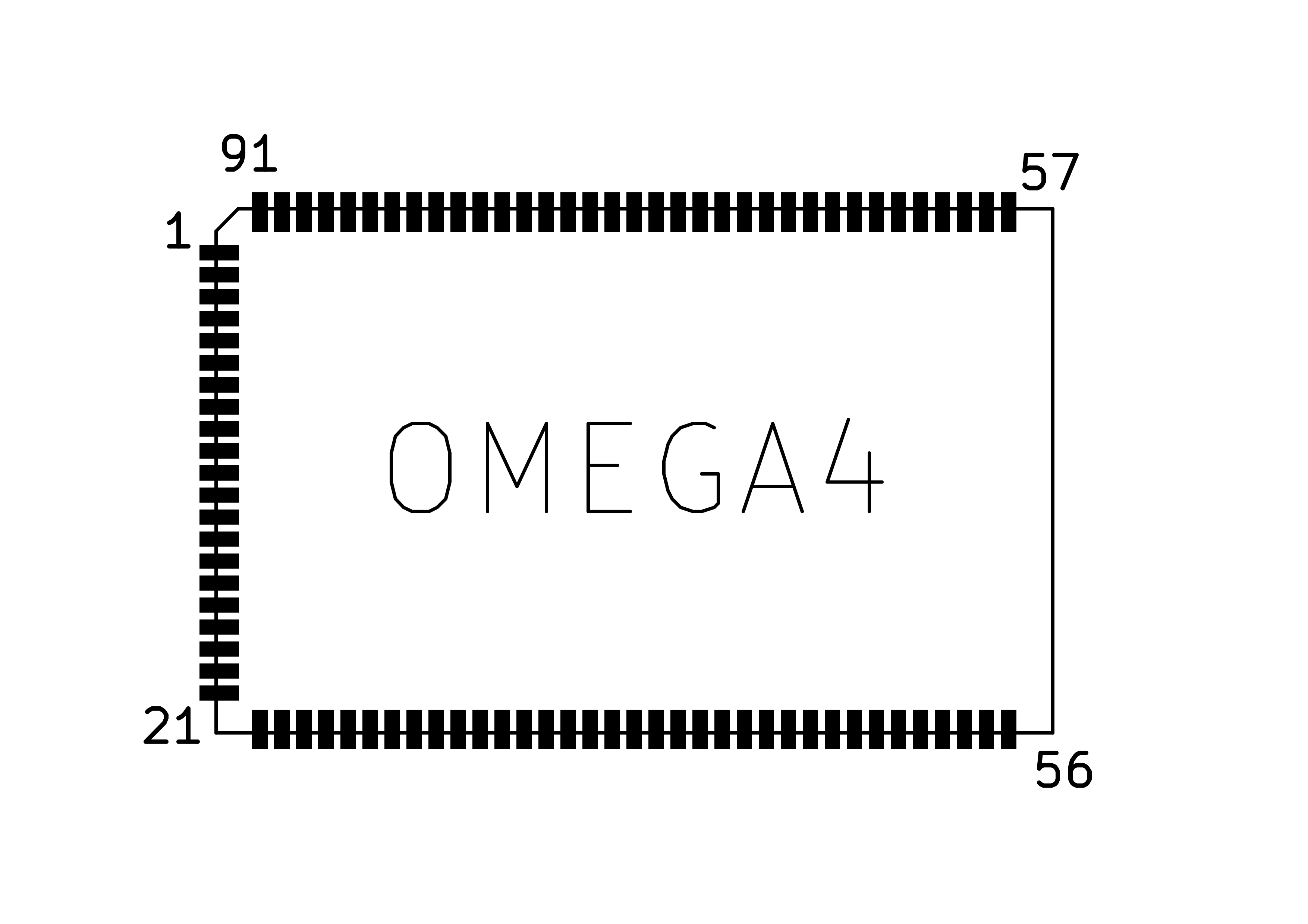
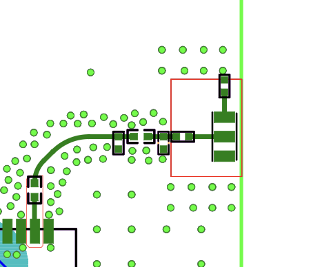
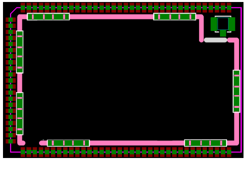
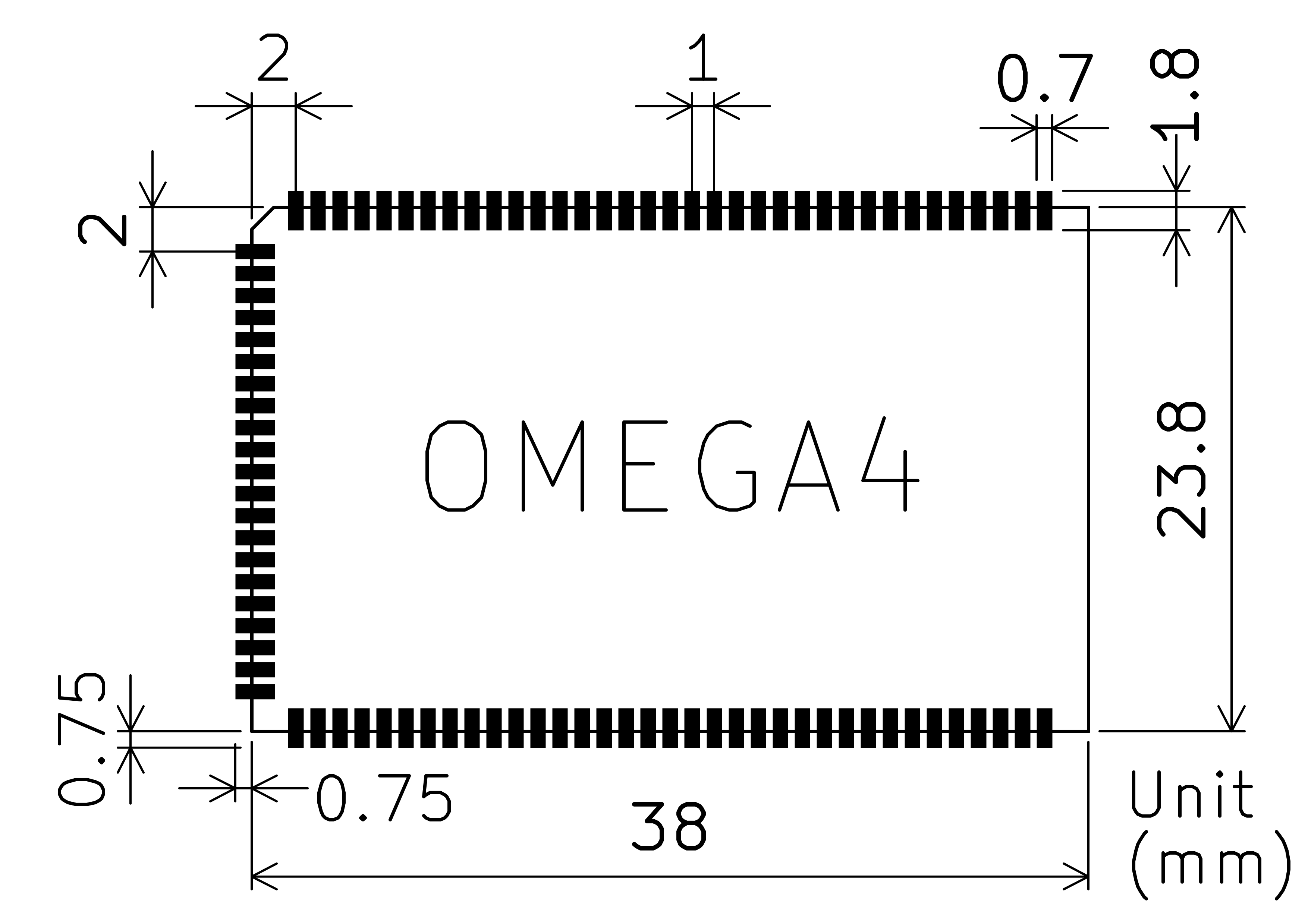
5.1 Omega4 Footprint
5.2 Impedance of the PCB Line
For best signal integrity, control the impedance of the following traces:
RF trace: 50 ohm single-ended.
Add ground stitching vias along the RF trace to provide a solid return path.
USB D+/D- pair: 90 ohm differential.
5.3 Test Points
If your carrier PCB has enough space, add test points for key rails and signals (power, debug UART, and boot straps). A 2.0 mm or 2.54 mm pitch is typical.
6. Design Checklist
Use this checklist to review a carrier-board design before PCB layout freeze.
6.1 Power
- 5 V input supply can support worst-case load (see
Peak Current Requirementin Section 1.1), including any downstream peripherals powered from the carrier board. - Input decoupling is placed close to PIN23/PIN24 with a low-impedance ground return (Section 4.1).
- VCC_1V8/VCC_3V3 loads stay within the limits in Section 4.2.
- All external peripherals use the correct I/O voltage domain (1.8 V vs 3.3 V) and include level shifting where required (Section 4.7).
6.2 Boot, Recovery, and Debug
FSPI_D0(PIN29) is accessible via a test point or button and is not inadvertently held low during normal boot (Section 4.4).- UART debug access is available (for example, expose UART0 TX/RX plus GND on a header or test points).
- Key rails and reset/boot strap signals have test points for manufacturing and bring-up (Section 5.3).
6.3 RF
- Only one RF path is active: either the on-module U.FL connector or
WL_ANT(PIN58) (Section 4.9). - RF trace impedance is controlled (50 ohm) and the RF keepout/grounding strategy is reviewed (Section 5.2).
6.4 High-Speed Routing
- USB D+/D- are routed as a 90 ohm differential pair with short stubs and good reference plane continuity (Section 4.10 and Section 5.2).
- MIPI-CSI routing, connector placement, and return paths are reviewed (Section 4.7).
- Ethernet routing and magnetics/jack selection are reviewed (Section 4.8).
7. Bring-Up and Debug
7.1 Recommended Bring-Up Header
During early development, it is helpful to expose the following signals on an accessible header or test pads:
- UART console TX/RX and GND (use the UART pins indicated for debug in the pin table).
FSPI_D0(PIN29) test point for MaskROM entry.- 5 V input and a ground test point for current measurement.
7.2 First Power-On Procedure
- Power the carrier board from a current-limited bench supply at 5 V.
- Verify no shorts on the 5 V rail and check that the steady-state current is in a reasonable range relative to the
No-load Running Currentin Section 1.1 (peripheral load will increase this). - Verify the module boots with
FSPI_D0not asserted. - If a UART console is available, capture the boot log for baseline reference.
7.3 Recovery (MaskROM)
If the module does not boot due to firmware or storage issues:
- Assert
FSPI_D0(PIN29) low during boot to enter MaskROM programming mode (Section 4.4). - Use your flashing/recovery toolchain to reprogram the module.
- Remove the assertion and reboot to return to normal boot.